Union Cabinet Approves ₹1.27 Lakh Crore Semicon 2.0 Push for India’s Chip Manufacturin
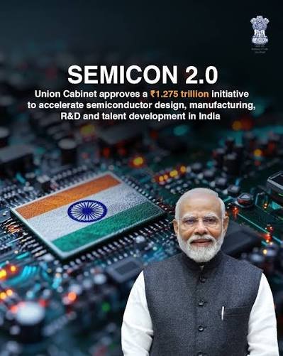
NEW DELHI: The Union Cabinet has approved the next phase of India’s semiconductor policy with a total outlay of ₹1,27,500 crore, expanding government support for chip design, manufacturing, packaging, research, equipment, materials and talent development. The approval for Semicon 2.0 was given on July 15, 2026, according to the Prime Minister’s Office.
The figure is substantially higher than the ₹15,000 crore cited in some descriptions of the policy. The official Cabinet announcement confirms that the total Semicon 2.0 budget is ₹1,27,500 crore.
Union Cabinet Semiconductor Scheme Expands Beyond Chip Fabs
The Union Cabinet Semiconductor Scheme is structured around six areas: chip design; machines and materials; additional fabrication plants; advanced ATMP and OSAT packaging facilities; research and development; and talent development.
The government says the programme builds on Semicon 1.0, which was approved in December 2021 with an outlay of ₹76,000 crore. That first phase focused heavily on establishing semiconductor fabrication and packaging capacity, while the new phase seeks to cover more parts of the supply chain.
The India Semiconductor Mission is therefore moving from initial manufacturing support to a broader industrial framework. The policy also aims to increase domestic capabilities in equipment, materials and semiconductor research, areas that are critical to building a complete production ecosystem.
Chip Manufacturing India Push Gets A Wider Supply-Chain Focus
The Chip Manufacturing India strategy extends beyond the fabrication of silicon wafers. Semicon 2.0 includes support for companies involved in semiconductor machinery, materials, chemicals and gases, alongside new fabs and more advanced packaging facilities.
The government said the first semiconductor fab is scheduled for commissioning in 2028. Under the programme, additional projects are expected to cover silicon fabs, compound semiconductor facilities, discrete components and display-related manufacturing.
The policy also addresses chip design. The Cabinet says 105 startups and micro, small and medium enterprises have received access to industry-standard electronic design automation tools, while 24 semiconductor design projects have been approved for financial support.
India Semiconductor Mission Builds On Early Projects
The India Semiconductor Mission has already approved 12 semiconductor manufacturing units with cumulative investment of more than ₹1.64 lakh crore, according to the government. Three companies — Micron, Kaynes and CG Semi — have started commercial production.
The broader electronics market is another part of the demand picture, with chips increasingly central to products ranging from automobiles and telecom equipment to flagship smartphones.
What Semicon 2.0 Means For India’s Electronics Ecosystem
The Union Cabinet Semiconductor Scheme is intended to reduce supply-chain dependence while increasing domestic manufacturing, design capability and specialised technical skills.
The government says around 68,000 students have already received semiconductor-related training through 315 universities under earlier efforts, while the next phase will expand training in areas such as clean-room operations, fabrication and semiconductor ecosystem construction.
For Chip Manufacturing India, the policy marks a shift from establishing individual facilities to building a wider chain covering design, production, packaging, equipment, research and skilled manpower.
The Cabinet’s July decision is now being implemented as India seeks to expand its role across the global semiconductor value chain. The confirmed policy outlay remains ₹1,27,500 crore, with the programme spanning the full semiconductor ecosystem rather than a single chip-manufacturing incentive.